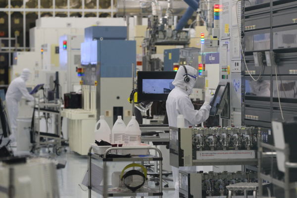
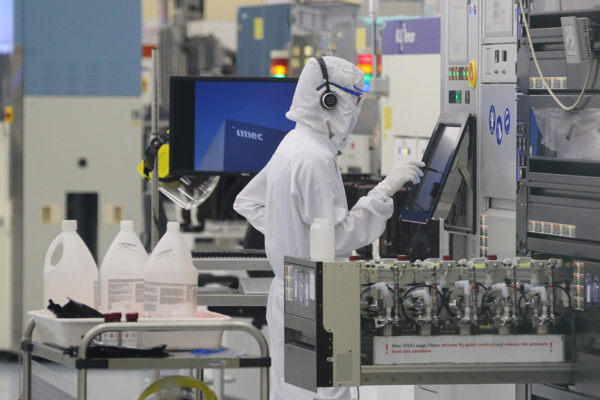
Imec achieves major progress in development of next-generation transistor technology

Flemish nanotechnology centre imec has made significant progress in the development of 2D materials for use in next-generation chips. It is presenting the results of its research, conducted in collaboration with chipmakers TSMC and Intel, at the IEEE International Electron Devices Meeting in San Francisco on Wednesday.
The number of transistors on a single chip has surged over recent decades, allowing chips to process more data at higher speeds on ever smaller surfaces. But the miniaturisation of traditional silicon technology is increasingly approaching its physical limits, while demand for chips continues to grow, driven in part by the rise of artificial intelligence.
Researchers have therefore been searching for alternatives for years. One of the most promising avenues is the use of 2D materials, which are just one or a few atomic layers thick. Imec believes they are one of the most promising candidates to replace silicon channels in future transistors.
But the extreme thinness of these materials also makes it incredibly challenging to use them to create chips, according to imec. "It is technically extremely difficult to apply such thin layers uniformly to silicon wafers and integrate them into existing manufacturing processes," the Leuven-based nanotechnology centre said in a press release.

2D transistor breakthroughs
Together with the Taiwanese semiconductor manufacturer TSMC and US technology company Intel, imec researchers have now tackled several of these challenges. They developed p-type transistors based on tungsten diselenide, known as WSe2.
"These 2D transistors deliver record performance and are fabricated using a process compatible with existing chip manufacturing, demonstrating the potential of 2D materials for future chip architectures," imec says in the press release.
At the same time, the researchers succeeded in scaling up the 2D materials to 300 mm wafers, the standard size used in mass chip production. The results indicate strong potential for industrial application at that scale as well, imec concludes.
#FlandersNewsService | © BELGA PHOTO BENOIT DOPPAGNE
Related news